In this story · 3 sections
For most of the last decade, the semiconductor conversation had a single protagonist: the lithography machine. The smaller the feature, the better the chip, and the fewer companies able to make the machine, the more geopolitical weight it carried.
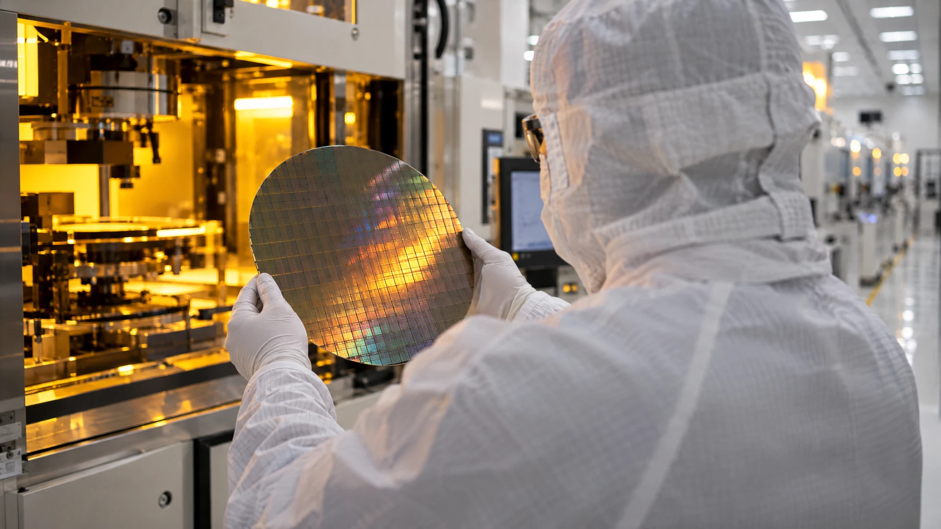
That story is still true, but it is no longer the whole story. As chips became collections of specialised dies rather than one monolithic slab, the difficult part moved downstream. Packaging — the business of connecting dies to each other and to the outside world — became a bottleneck in its own right.
Why packaging matters now
A modern AI accelerator is less a single chip than a small city of chiplets. Compute dies sit next to memory stacks, connected by microscopic pathways. The performance of the whole depends on how well those connections are made, and how much heat the arrangement can survive.
The companies that can package at scale are few. Capacity is booked years ahead. A shortage of packaging capacity does not stop wafers being made, but it stops them becoming products.
You can print a wafer in weeks. You cannot conjure a qualified packaging line in months.
Memory is the other queue
High-bandwidth memory has its own constraints. It is stacked, tested and qualified in a small number of facilities. Demand from AI systems has pulled capacity away from other markets, which is why memory prices have become a subject of board-level concern.
This is an old pattern in the industry: a component that was once a commodity becomes strategic when the architecture changes. The difference is speed. Previous cycles gave buyers a year or two to adapt. This one has given them quarters.
Analysis
What to watch
Look less at announced fab investment and more at qualification timelines. A new packaging line takes time to prove, not just to build. The companies that announce capacity are not always the companies that can use it.
The industrial answer
Governments have responded with subsidies for fabrication, but packaging has received less attention. That is beginning to change. Several regions are funding advanced packaging centres, partly for supply-chain resilience and partly because the work is a natural bridge between research and manufacturing.
The risk is that money arrives before the workforce does. Packaging is a discipline of process, patience and tacit knowledge. It is not easily transplanted.
None of this means the chip shortage will return in its old form. It means the constraint has become more distributed, and therefore harder to see. The industry’s next bottleneck will not be a single machine. It will be a set of skills, facilities and relationships that take longer to build than any factory.




Join the conversation
0 commentsNo comments yet. Add a considered thought — comments are moderated by the editors.